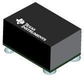
SN74LVC1G79YZPR, Flip Flops Sngl+EdgeTrggrd DTypeFlipFlop

Изображения служат только для ознакомления,
см. техническую документацию
см. техническую документацию

120 руб.
от 10 шт. —
100 руб.
от 100 шт. —
76 руб.
от 500 шт. —
65.61 руб.
Добавить в корзину 1 шт.
на сумму 120 руб.
Описание
Semiconductors\Logic ICs\Flip Flops
SN74LVC1G79/SN74LVC1G79-Q1 D-Type Flip-FlopTexas Instruments SN74LVC1G79/SN74LVC1G79-Q1 Single D-Type Flip-Flop is designed for 1.65V to 5.5V V CC operation. When data at the data (D) input meets the setup time requirement, the data is transferred to the Q output on the positive-going edge of the clock pulse. Clock triggering occurs at a voltage level and is not directly related to the rise time of the clock pulse. Following the hold-time interval, data at the D input can be changed without affecting the level at the output. The SN74LVC1G79 is fully specified for partial-power-down applications using I off. The I off circuitry disables the outputs when the device is powered down. This feature inhibits current backflow into the device which prevents damage to the device. The SN74LVC1G79-Q1 devices are AEC-Q100 qualified for automotive applications.
Технические параметры
| Brand: | Texas Instruments |
| Factory Pack Quantity: Factory Pack Quantity: | 3000 |
| Function: | D-Type |
| High Level Output Current: | -32 mA |
| Input Type: | CMOS, TTL |
| Logic Family: | LVC |
| Logic Type: | True |
| Low Level Output Current: | 32 mA |
| Manufacturer: | Texas Instruments |
| Maximum Operating Temperature: | +125 C |
| Minimum Operating Temperature: | -40 C |
| Mounting Style: | SMD/SMT |
| Number of Channels: | 1 Channel |
| Number of Circuits: | 1 |
| Number of Input Lines: | 1 |
| Number of Output Lines: | 1 |
| Operating Supply Voltage: | 1.8 V, 2.5 V, 3.3 V, 5 V |
| Operating Temperature Range: | -40 C to+125 C |
| Output Type: | Single-Ended |
| Package / Case: | DSBGA-5 |
| Polarity: | Non-Inverting |
| Product Category: | Flip Flops |
| Product Type: | Flip Flops |
| Propagation Delay Time: | 5 ns |
| Quiescent Current: | 10 uA |
| Series: | SN74LVC1G79 |
| Subcategory: | Logic ICs |
| Supply Voltage - Max: | 5.5 V |
| Supply Voltage - Min: | 1.65 V |
| EU RoHS | Compliant |
| ECCN (US) | EAR99 |
| Part Status | Active |
| Logic Family | LVC |
| Logic Function | D-Type |
| Number of Channels per Chip | 1 |
| Number of Elements per Chip | 1 |
| Number of Element Inputs | 1 |
| Number of Element Outputs | 1 |
| Bus Hold | No |
| Polarity | Non-Inverting |
| Triggering Type | Positive-Edge |
| Maximum Propagation Delay Time @ Maximum CL (ns) | 5@3.3V|4.5@5V |
| Absolute Propagation Delay Time (ns) | 9.9 |
| Process Technology | CMOS |
| Input Signal Type | Single-Ended |
| Maximum Low Level Output Current (mA) | 32 |
| Maximum High Level Output Current (mA) | -32 |
| Minimum Operating Supply Voltage (V) | 1.65 |
| Typical Operating Supply Voltage (V) | 5|3.3|2.5|1.8 |
| Maximum Operating Supply Voltage (V) | 5.5 |
| Maximum Quiescent Current (mA) | 0.01 |
| Propagation Delay Test Condition (pF) | 50 |
| Minimum Operating Temperature (°C) | -40 |
| Maximum Operating Temperature (°C) | 85 |
| Packaging | Tape and Reel |
| Standard Package Name | BGA |
| Pin Count | 5 |
| Supplier Package | DSBGA |
| Mounting | Surface Mount |
| Package Height | 0.31(Max) |
| Package Length | 1.42(Max) |
| Package Width | 0.92(Max) |
| PCB changed | 5 |
| Lead Shape | Ball |
| Вес, г | 0.01 |
Дополнительная информация
Калькуляторы группы «Логические - Триггеры»
Типы корпусов импортных микросхем


