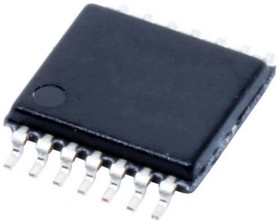
CD4066BPWR, Analog Switch ICs Quad

Изображения служат только для ознакомления,
см. техническую документацию
см. техническую документацию

130 руб.
от 10 шт. —
99 руб.
от 100 шт. —
70 руб.
от 500 шт. —
55.56 руб.
Добавить в корзину 1 шт.
на сумму 130 руб.
Описание
Semiconductors\Switch ICs\Analog Switch ICs
CD4066B Quad Bilateral SwitchTexas Instruments CD4066B Quad Bilateral Switch is intended for the transmission or multiplexing of analog or digital signals. The device is pin-for-pin compatible with the CD4016B but exhibits a much lower on-state resistance. The on-state resistance is also relatively constant over the full signal-input range. The CD4066B device consists of four bilateral switches, each with independent controls. Both the p and the n devices in a given switch are biased on or off simultaneously by the control signal. The well of the n-channel device on each switch is tied to either the input (when the switch is on) or to V SS (when the switch is off). This configuration eliminates the variation of the switch-transistor threshold voltage with input signal and keeps the on-state resistance low over the full operating-signal range.
Технические параметры
| Brand: | Texas Instruments |
| Configuration: | 4 x SPST |
| Factory Pack Quantity: Factory Pack Quantity: | 4000 |
| Manufacturer: | Texas Instruments |
| Maximum Dual Supply Voltage: | +/-7.5 V |
| Maximum Operating Temperature: | +125 C |
| Minimum Dual Supply Voltage: | +/-7.5 V |
| Minimum Operating Temperature: | -55 C |
| Mounting Style: | SMD/SMT |
| Number of Channels: | 4 Channel |
| Off Time - Max: | 30 ns |
| On Resistance - Max: | 240 Ohms |
| On Time - Max: | 30 ns |
| Package / Case: | TSSOP-14 |
| Product Category: | Analog Switch ICs |
| Product Type: | Analog Switch ICs |
| Series: | CD4066B |
| Subcategory: | Switch ICs |
| Supply Current - Max: | 5 uA |
| Supply Type: | Single Supply, Dual Supply |
| Supply Voltage - Max: | 18 V |
| Supply Voltage - Min: | 3 V |
| Automotive | No |
| Chip Enable Signals | Yes |
| Configuration | Quad SPST |
| ECCN (US) | EAR99 |
| EU RoHS | Compliant |
| Input Signal Type | Single |
| Lead Shape | Gull-wing |
| Maximum Dual Supply Voltage (V) | ±9 |
| Maximum Frequency (25°C) @ Vcc (MHz) | 40(Typ)@±5V |
| Maximum On Resistance (Ohm) | 1050@5V |
| Maximum On Resistance Range (Ohm) | >=1000 |
| Maximum Operating Temperature (°C) | 125 |
| Maximum Propagation Delay Bus to Bus (ns) | 15@15V|20@10V|40@5V |
| Maximum Single Supply Voltage (V) | 18 |
| Maximum Turn-Off Time (ns) | 70@5V |
| Maximum Turn-On Time (ns) | 70@5V |
| Minimum Dual Supply Voltage (V) | ±1.5 |
| Minimum Operating Temperature (°C) | -55 |
| Minimum Single Supply Voltage (V) | 3 |
| Mounting | Surface Mount |
| Number of Channels per Chip | 4 |
| Number of Inputs per Chip | 4 |
| Number of Outputs per Chip | 4 |
| Output Signal Type | Single |
| Packaging | Tape and Reel |
| Part Status | Active |
| PCB changed | 14 |
| Pin Count | 14 |
| Polarity | Non-Inverting |
| Power Supply Type | Single|Dual |
| PPAP | No |
| Propagation Delay Test Condition (pF) | 50 |
| Standard Package Name | SOP |
| Supplier Package | TSSOP |
| Supplier Temperature Grade | Military |
| Switch Architecture | SPST |
| Type | Analog Switch |
| Typical Dual Supply Voltage (V) | ±3|±5 |
| Typical Single Supply Voltage (V) | 5|9|12|15 |
| Вес, г | 0.0572 |
Техническая документация
Datasheet CD4066BPWR
pdf, 1430 КБ
Datasheet CD4066B
pdf, 1517 КБ
Дополнительная информация
Калькуляторы группы «Аналоговые коммутаторы, Мультиплексоры, Демультиплексоры»
Типы корпусов импортных микросхем


